DC Transformer
By Ken Kranz
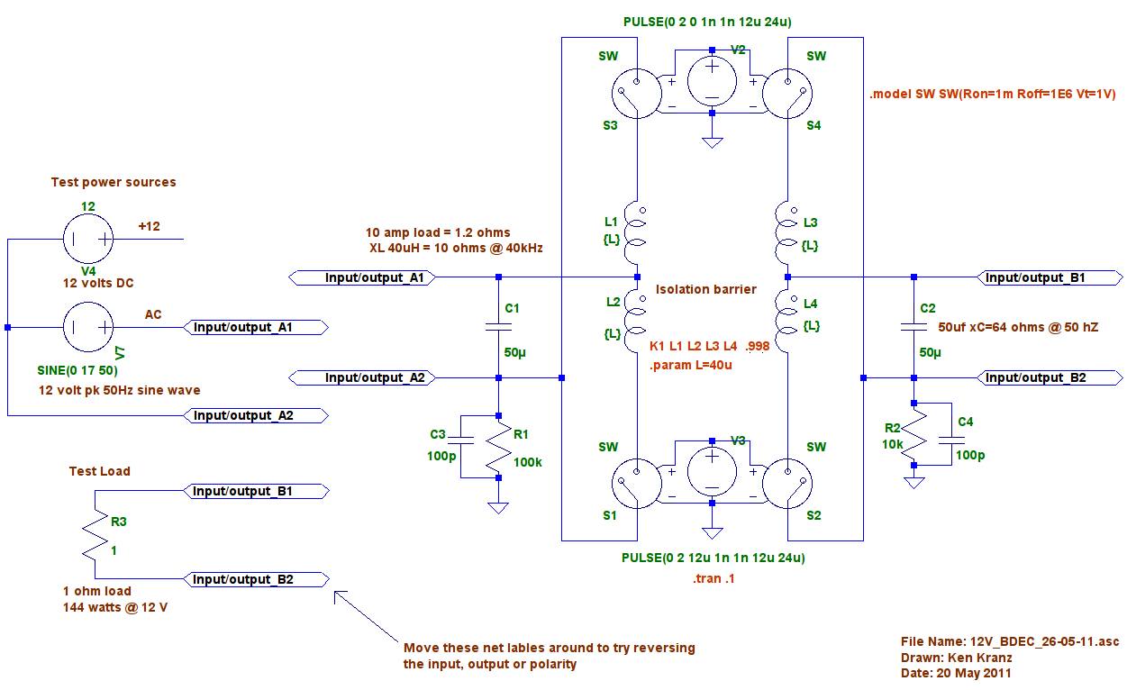
Of course such a thing does not exist, I do however have your attention. It is sometimes a requirement to have two lead acid batteries connected in parallel allowing power to flow in either direction between them while maintaining galvanic isolation. A good example of this is trying to close the loop on some of the claimed over unity devices. The image below shows how the power into a transformer may be switched converting the DC input into high frequency AC to allow it to pass through a high frequency transformer. The output of the transformer is synchronously rectified to restore the DC. As drawn (Fig 1) the operation is bidirectional and power may flow in either direction, the input/output polarity is also unimportant as even low frequency AC may pass through the device.

Fig 1; zip includes Figs 1, 2, 3 and spice files for same
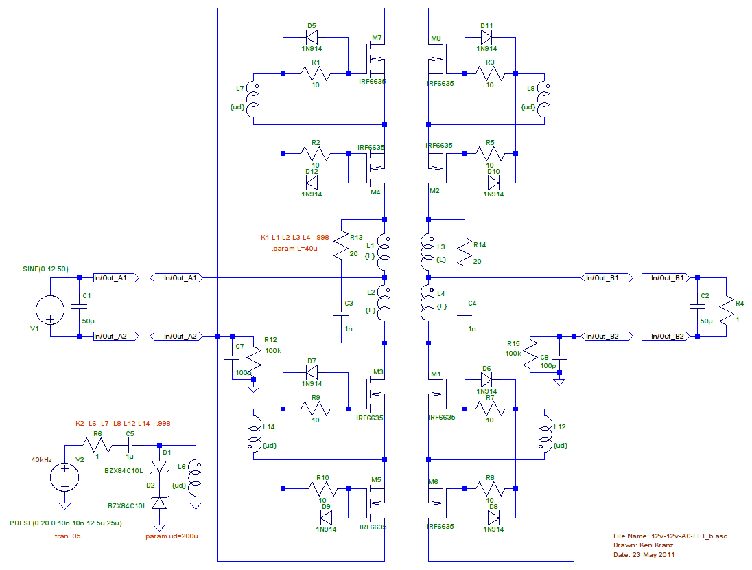
Using this type of technology it would be possible to make a 220 VAC to 220 VAC isolation transformer using lightweight ferrite cores running at high frequency rather than a conventional steel core running at 50 Hz. When running the spice simulation the inputs and outputs from can be swapped around in any polarity and the device will work. Two input signals have been set up, a 12 volt DC supply and a 50 Hz 12volt peak sine wave. C3, R1, R2, C4 are in place to enable the simulator to operate. The simulation is simplistic and is designed to show the operating principal. Evil parasitic capacitances and less than perfect parts are not shown. Below is an image of something a little more realistic (Fig 2) using actual semiconductor switching. It is not for construction, only to show a possible topology that allows DC or low frequency AC to pass through the device.

Fig. 2
The next schematic (Fig 3) is of a full bridge configuration DC 0 to 12 volts input. The full bridge allows for better transformer coupling than the center tapped design. Inter-winding capacitance and other evil's are not shown. Disadvantages include more FET gates to drive and more FET series resistance.

Fig. 3
Fig. 4 is of something more likely to be built, indeed we something similar working! The fact that all gates require only low side drivers is attractive as cheap high current drivers are available. High speed digital isolators that work like super fast opto couplers solve the problem of drive signal across the isolation barrier. The digital isolators offer low capacitance, high voltage isolation and high speed. The simulation has transformer gate drive, this is for illustrative purposes only. Capacitance across the isolation barrier is often a problem with gate drive transformers. The capacitance of the main power transformer is unavoidable. One of the design challenges is how the device powers up. Will it be required to start regardless of power into side A or side B ? Once running it will not matter. During start up the parasitic diodes across the FET's on the unpowered side act as rectifiers, this can produce the required start up voltage for the unpowered side. Our working prototype functions in this manner. Another possible method would be to have control and drive circuitry on both sides A and B with first up having control. Some sort of low voltage lock out may be required depending on where the control and gate drive power is derived from. If an external power supply is used for the gate drive, operation will all the way down to zero volts.

Fig. 4
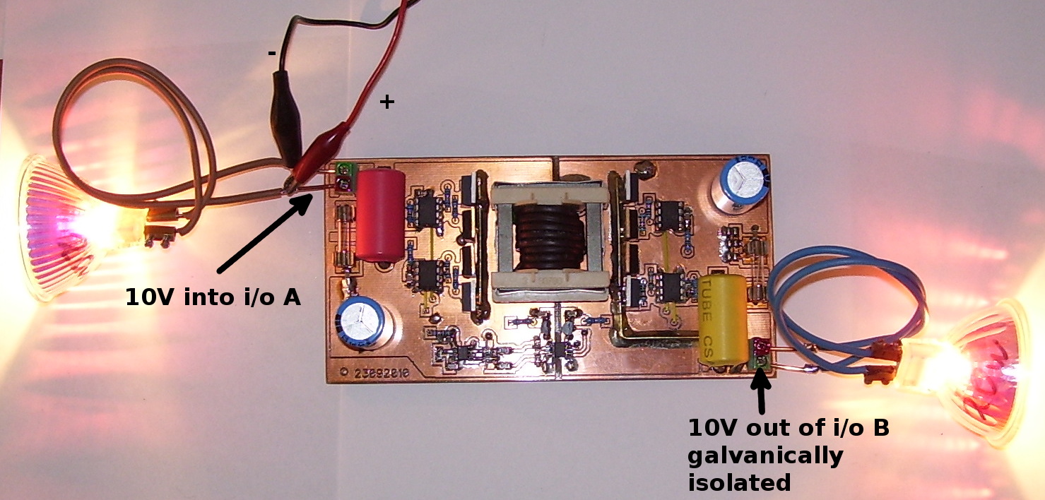
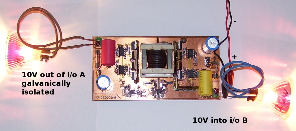
The images below are of an experimental BDEC (Bi Directional Energy Conduit) similar in topology to Fig 4 it uses 8 IRF3205 FET's, 6 amp microchip gate drive IC's, a high speed digital isolator and a single chip frequency generator, it was routed using a small CNC mill as are most of our experimental/prototype boards.

Image 1 The BDEC running with power applied to side A. Ten volts was used to reduce lamp brilliance.

Image 2 The BDEC running with 10 volts applied to side B, a jump start was required as the oscillator chip is on side A.

Image 3 The BDEC running from a 12 volt battery with side B connected in series with the input to produce a DC voltage doubler. The two 12 volt lamps are in series and connected across the 24 volt supply.
About the transformer windings, even at the run frequency of 37662 Hz skin effect is a problem. The black wire you see is actually heat shrink tubing over two strands of enamel coated wire treated as a single conductor. Six separate interleaved windings are used to reduce the leakage inductance and resistance. The winding is not ideal, it is hard to hand wind a good transformer, the insulation between the two windings needed to be suitable for the intended purpose as did the creepage distances. At 12.6 volts in the flux density is about 2000 gauss. A high permeability low loss core material should be used. F5A was used as the core is a stock item. This device was for testing purposes, many design changes will be made for the next version. With 5 amp fuses fitted and a 20 watt load the voltage drop across the fuses is greater than the voltage drop through the device. Ten amp fuses were fitted even for low powered testing to reduce this problem. Fuse types with very low series resistance will need to be investigated. Some tests carried out on the experimental board. The input current with no load on i/o #2 was 180mA (2.28 watts). The dominant overheads were the transformer magnetising current and gate drive requirements. This could be improved. With 12.6 volts into i/o #1 the output voltage on i/o #2 measured 12.599 volts (down 1mV). With 12.6 volts into i/o #1 and a 20 watt lamp on i/o #2 the output voltage measured 12.533 (down 67mV). With 12.6 volts into i/o #1 and a 50 watt lamp on i/o #2 the output voltage measured 12.433 (down 167mV). A 50 watt lamp was fitted to the output 12.6 volts was fed into i/o #1. current was 4.23 amps therefore input power was 53.298 watts, the output power was 50.56 watt, therefore the efficiency was 94.8% . Considering the 2.28 watts zero load current this is not two bad, actually seems to good will have to redo this test. All test revealed the equivalent series pass resistance was less than .045 ohms. The measurements were made with a Fluke 75 multimeter. When taking the voltage drop measurement the voltages were taken across the input/output capacitors to exclude the fuse voltage drop. A verification was to jumper the negative side of both i/o capacitors and measure the voltage from capacitor to capacitor positive. A more precise series of tests could be carried out, it may not happen as the concept seems reasonably sound and a pre production design may be undertaken if there is enough interest. As we all can see no heatsinks are required so SMD FET's should be used very close or under the transformer.

Image 4
C Capacitors i/o filter D 6 amp gate drive IC's F Fuses Fe Ferrite Sleeve i The isolation barrier in the PCB i/o A Input/output A i/o B Input/output B O Oscillator IC P Power FET's T High frequency transformer W Transformer windings
About the transformer windings, even at the run frequency of 37662 Hz skin effect is a problem. The black wire you see is actually heat shrink tubing over two strands of enamel coated wire treated as a single conductor. Six separate interleaved windings are used to reduce the leakage inductance and resistance. The winding is not ideal, it is hard to hand wind a good transformer, the insulation between the two windings needed to be suitable for the intended purpose as did the creepage distances. At 12.6 volts in the flux density is about 2000 gauss. A high permeability low loss core material should be used. F5A was used as the core is a stock item. This device was for testing purposes, many design changes will be made for the next version. As the coupling coefficient of the transformer goes up so does the capacitance between the input and output, how much capacitance is acceptable? With 5 amp fuses fitted the voltage drop across the fuses is greater than the voltage drop through the device. Ten amp fuses were fitted even for low powered use to reduce this problem. Fuse types with low series resistance will need to be investigated. Future Development A BDEC using back to back variable regulated supplies with microprocessor control has been investigated. The topology offers enhanced operation with exceptionally low voltage drop through the device and larger i/o voltage ranges. Flyback converters could then be used. The main disadvantages are the cost and complexity. End
Copyright © 2026. Chava Science.